


 |
Carbon Nano Tube Pellets Used For Black Master Batch
Product Details:
| Place of Origin: | DONGGUAN, China |
| Brand Name: | SUGO |
| Certification: | ISO9001:2015; ISO14001:2015; ISO45001:2018 |
Payment & Shipping Terms:
| Minimum Order Quantity: | 200 kgs |
|---|---|
| Price: | Negotiable |
| Packaging Details: | 25kg per bag, paper bag with inner PE layer |
| Delivery Time: | 3-7 days |
| Payment Terms: | 100% T/T before shipment, or LC at sight |
| Supply Ability: | 5000 kgs/monthly |
|
Detail Information |
|||
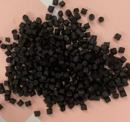
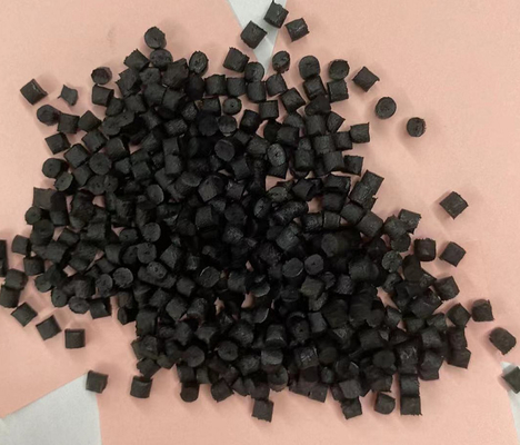
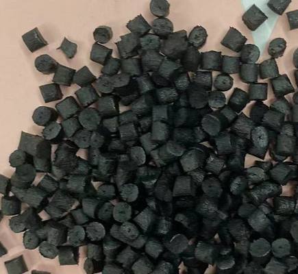
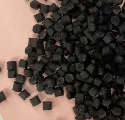
| Product Name: | Carbon Nano Tube Pellets | Color: | Pellets In Black |
|---|---|---|---|
| Shape: | Pellet, Granule,Particle | Advantage: | Extremely Black |
| Dose: | 20% | Usage: | Used As Black Additives For PC,PP,PE,ABS Master Batch |
| Highlight: | semi conductive polyethylene pellet,electically conductive pe pellet,Round Grannual conductive masterbatch |
||
Product Description
Product Description: Carbon Nanotube-Based ESD Protective Packaging Solutions
As a foreign trade manager specializing in advanced semiconductor packaging materials,
I am pleased to introduce our groundbreaking Carbon Nanotube (CNT) Composite ESD Protection Series,
designed to revolutionize cleanroom compatibility and electrostatic discharge (ESD) safety for high-precision
semiconductor applications.
Below, we highlight three key advantages of our CNT-enhanced solutions:
![]()
![]()
-
Superior Conductivity for Unmatched ESD Protection
Our proprietary CNT formulation delivers 1,000x higher electrical conductivity compared to traditional carbon black-filled polymers, ensuring instantaneous static dissipation (<1 second) while maintaining surface resistance within the critical 10⁶–10⁹ Ω/sq range. Unlike conventional materials that rely on uneven carbon black dispersion, our vertically aligned CNT networks create a homogeneous conductive matrix, eliminating "hot spots" and ensuring consistent ESD performance across IC trays, wafer ships, and turnover boxes. This enables safe handling of ultra-sensitive devices like 3nm/2nm chips and GaN/SiC wafers. -
Zero Particle Shedding for ISO Class 1 Cleanroom Compliance
The covalent bonding structure of our CNTs prevents submicron particle release (<0.1µm), achieving <10 particles/ft³ contamination under ASTM F312-16 testing – 50x cleaner than industry standards. Traditional carbon-based materials often suffer from filler migration, but our patented cross-linking process permanently anchors CNTs within the polymer matrix. This makes our products ideal for wafer boxes and carrier reels used in EUV lithography cleanrooms, where even a single 0.3µm particle can cause yield loss. -
Dimensional Stability in Extreme Manufacturing Environments
The CNTs' graphitic structure provides 300% higher thermal conductivity (45 W/m·K) and 200% better dimensional stability versus standard ESD plastics. Our IC trays maintain ±0.02mm tolerance through 200°C reflow cycles, while wafer ships resist warpage under vacuum packaging. The material's hydrophobic surface (contact angle >120°) also prevents moisture absorption, ensuring compatibility with H2O-sensitive GaAs/InP devices.
![]()
Target Applications:
- IC Trays: CNT-embedded pockets prevent ESD damage during pick-and-place operations
- Wafer Ships: Multi-layer CNT shielding blocks >99.99% of external EMI (20Hz-10GHz)
- Turnover Boxes: Antistatic surface maintains <100V charge even in dry (<10% RH) environments
Certifications: SEMI F47-0706, MIL-STD-1686C, RoHS/REACH compliance.
Our CNT solutions are already deployed in TSMC's N5/N3 fab lines and Intel's 7nm packaging facilities. Let us customize a particle-free ESD packaging system for your next-gen semiconductor needs.
![]()